![]() FUNCTIONAL MATERIAL SURFACE OBSERVATION AND MEASUREMENT
FUNCTIONAL MATERIAL SURFACE OBSERVATION AND MEASUREMENT
UNDER PHASE=SHIFT EUV MICROSCOPE
![]() EVALUATION AND DEVELOPMENT OF EXPOSURE SYSTEM FOR EUVL
EVALUATION AND DEVELOPMENT OF EXPOSURE SYSTEM FOR EUVL
![]() DEVELOPMENT OF DIGITAL IMAGING RESIST FOR NANO DEVICE
DEVELOPMENT OF DIGITAL IMAGING RESIST FOR NANO DEVICE
FUNCTIONAL MATERIAL SURFACE OBSERVATION AND
MEASUREMENT UNDER PHASE-SHIFT EUV MICROSCOPE
We have a technological subject called defect-free mask fabrication for the realization of EUVL, we need to inspect the defect with 30nm size at high speed by 2007 put in practical use. For the reason we proceed the development of Phase-Shift EUV Microscope as a tool which can observe phase defect because of multilayer deposition and amplitude defect of mask.
It is the purpose to build what can obtain the 3D-Xray image of 6000 magnifications power and 20nm wide and 0.03nm high in resolution , and to advance analysis of the surface and the interface of a multilayer film, and to clarify reason for non-defect of a mask.
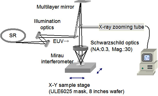
PASE-SHIFT EUV MICROSCOPE
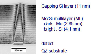
Phase defect.
We set a goal to observe such as phase defect that we couldn't find out
in usual method of mask inspection.
Specification of observation.
The contrast go up per 10 seconds.
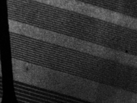
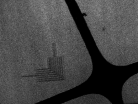
Observation result of the mask for EUVL..
click here for questions etc.
![]()
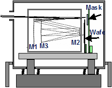
The system of the following figure was carried forward as joint research with Hitachi Central Research Laboratory and NIKON from 1996, and development was furthered as joint research with ASET from October, 1998.
EVALUATION AND DEVELOPMENT OF EXPOSURE SYSTEM FOR EUVL
In our Laboratory, we have proceeded the research on EUVL since 1984. The system of the following figure was carried foward as joint reseach with Hitachi Central Research Laboratory and NIKON from 1996, and development was furthered as join research with ASET from October, 1998. In autumn of 1999, we succeeded pattern replication of fine pattern 56nm. Moreover we succeeded in large-field exposure which have fine pattern of 60nm within 10mm×10mm range in 2001.
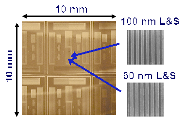
Exposure system (ETS-1) Large-field exposure pattern using ETS-1
![]()
DEVELOPMENT OF DIGITAL IMAGING RESIST FOR NANO DEVICE
In the feauture of IT indusry, the development of electronic devices, which
is possible to process with dozens of GHz high speed and low drive electric
power of not more than 1V is expected.
The mass production of a device with 32 nm class of line width is scheduled
for 2009. Furthermore, quantumn device requires fine processing of 10nm
or less.
In the line width of dozens of nm or less, since it is equivalent to
some molecules , the line width control equivalent to one molecule would
be a subject.
Then, a reaction needs to progress at high efficiency to one light , and it is necessary to develop a digital imaging resist (DIR) which reaction progresses in the only irradiation area by self-organization.
In the development of EUVL technology, we had been proceeding evaluation
of the resist which has low-outgassing and low LER. Forthermore, we'bee
proceeding the development of digital imaging resist.
click here for questions etc.
![]()
Since the EUV light which is near the wavelength 13.5nm has strong absorption of a substance and the index of refraction is close to 1, a lens of transmission type cannot be used for an optics. Therefore reflective optics was required, however, in a direct incidence optics which is few to aberration, a thin film which obtains high reflectance did not exsist.
As a method of improving it, the development of multilayer which is carried
out two kinds of optical ultla-thin films to dozens of layers by turns,
and used by interference of the reflective lights from each layer.
We're proceeding multilayer deposition of Mo/Si which can obtain high reflectance
with the light (13.5nm) used for EUVL.. Moreover, manufacture of beam spritter
which is indispensable under the phase -shift EUV microscope is also advanced.
And we proceed multilayer deposition by magnetron sputter system.
Measurement of multilayer reflectivity is performed by NewSUBARU BL10.
60%or more of reflectance is obtained by direct incident with the Mo/Si
multilayer film.
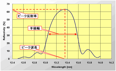
Reflectivity of multilayer on mask for EUVL (HOYA)
![]()
Although EUV lithography is performed in a vacuum, while continuing exposure, a contamination (mainly carbon) adheres to an optics, a mask etc, of exposure system. A contamination reduces reflectivity and the throughput of exposure. The gas, which comes out of equipment and occurs from a resister during exposure, are one of the causes of contamination adhesion.
Now, in this lablratory, we're examaing the following things to the problem
of a contamination.
(1) reduce the outgas that is the source of contamination from the equipment
and resist.
(2) remove the contamination adhering to the optics.
Especially about (2), we propose the method of removing it by passing oxygen into the vacuum chamber during exposure, and the method of using the 172nm light from Xeeximer lamp as efficiently method.
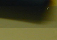
Contamination on the mask.
After removing it, reflectivity recovered.
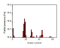
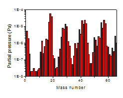
Outgassing species from SUS304 Outgassing species from shrink tube
Comparison of the outgassing quantity from the composion material in equipment
![]()